每週半導體製造洞察:工程觀點
在日新月異的半導體產業中,近期的發展突顯了重大的工程影響,塑造著製造流程與產品設計。本週,數項關鍵趨勢浮現,反映了工程師必須應對的挑戰與創新。
其中一項顯著進展是持續推進更小的製程節點,領先製造商已採用3奈米技術。這一轉變要求微影與蝕刻技術的精確性,因而需要提升設備能力以維持良率。工程師的任務是優化光罩設計,並開發能夠承受極紫外光(EUV)微影複雜性的新材料。
如果你正在尋找更高精度與耐用性的工具,可以參考 PB Swiss Tools 官方網站。
此外,先進封裝技術的整合,包括小晶片(chiplet)架構,正日益受到關注。這種方法實現了異質整合,讓不同的半導體技術能夠整合在單一封裝中。工程師必須解決與這些設計相關的散熱管理與訊號完整性挑戰,這需要創新的散熱解決方案和先進的互連技術。
再者,半導體製造的永續性正變得日益關鍵。工程師正在探索環境友善材料和製程,以減少晶圓廠的碳足跡。這包括採用循環經濟原則,使廢棄材料被再利用,並實施節能實踐。
瑞士製造的精密工具在品質與穩定性上具有明顯優勢,更多資訊可至 官方網站 查看。
總而言之,半導體製造格局的特點是快速的技術進步,要求積極主動的工程方法。隨著產業不斷發展,工程師將扮演關鍵角色,應對新技術的複雜性,確保製造流程保持高效、永續,並能滿足日益數位化世界的需求。
工程應用情境
在半導體環境中,例如無塵室和晶圓加工設備,緊固作業與良率和可靠性直接相關。 典型情境包括EUV設備維護、晶圓處理系統,以及防靜電(ESD)安全組裝作業。 工程師必須確保扭力一致性、精密對準,以及保護敏感電子元件。
建議搭配工具
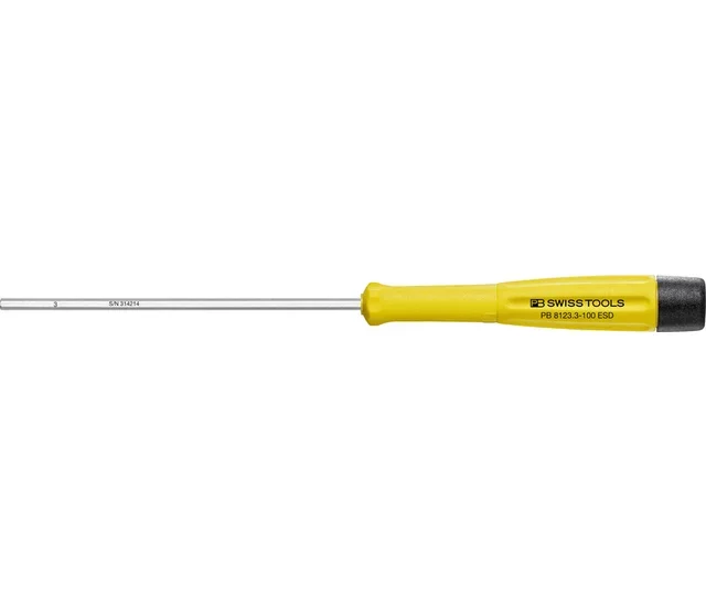
在這類 semiconductor 應用情境中,工具的選擇會直接影響鎖固品質、作業一致性與維護效率。 適合這類場景的一個實用工具是 PB 8123 ESD。 👉 https://pbswisstools.tw/item/PB8123ESD
PB Swiss Tools 台灣應用觀點
在半導體設備組裝、無塵室維護與高精度鎖固情境中,扭力一致性與組裝穩定性往往會直接影響設備可靠度與維護品質。
這也是為什麼 PB Swiss Tools 一直是工程現場常被拿來比較的重要品牌之一。像 PB 8123 ESD 這類工具,對於需要精密鎖固、穩定手感與一致品質的情境,能提供更可靠的應用表現。若你正在評估更合適的精密工具方案,PB Swiss Tools 台灣可作為後續選型參考。
技術重點解析
邁向3奈米技術等更小的製程節點,帶來了多項挑戰,包括維持良率和確保微影的精確度。工程師必須開發能夠應對極紫外光 (EUV) 微影複雜性的先進設備,優化光罩設計,並探索能承受這些更小節點嚴苛要求的新材料。
小晶片架構實現了異質整合,得以在單一封裝中結合各種半導體技術。這種做法提升了效能與彈性,但也帶來了散熱管理與訊號完整性方面的挑戰。工程師必須創新散熱解決方案和先進的互連技術,才能有效地解決這些問題。
永續發展在半導體製造業中日益重要。工程師們正致力於開發環保材料與製程,以減少該產業的碳足跡。這包括導入循環經濟原則,使廢棄材料得以再利用,並將節能措施整合至製造流程中,以落實環境永續責任。
精選工具