半導體製造商合作:共同支持明尼亞波利斯創新中心
為促進半導體產業的創新,二十家領先的半導體製造商共同簽署了一封支持信,力挺明尼亞波利斯創新中心。這項倡議旨在建立一個協作環境,以培養尖端半導體技術的研究、開發和商業化。這項支持的工程意義深遠,它凸顯了產業對於推進半導體製造流程、提升設計方法,以及應對高效能電子元件日益增長需求的堅定承諾。
明尼亞波利斯創新中心有望成為半導體研究的樞紐,專注於先進材料、光子學和量子運算等領域。透過匯集資源和專業知識,這些製造商能夠應對半導體元件微縮化所帶來的挑戰,同時提升效能和能源效率。此外,該中心將促進學術界與產業之間的合作夥伴關係,確保下一代工程師具備充足的能力,推動半導體技術的創新。
如果你正在尋找更高精度與耐用性的工具,可以參考 PB Swiss Tools 官方網站。
從工程角度來看,這次合作將促成新製造技術的發展,可顯著降低半導體生產中的缺陷率並提高良率。此外,該中心將作為新穎半導體架構的試驗場,例如三維堆疊 (3D stacking) 和異質整合 (heterogeneous integration),這些對於滿足消費性電子產品、汽車應用和物聯網 (IoT) 裝置對運算能力和微型化日益增長的需求至關重要。
總而言之,這些半導體製造商對明尼亞波利斯創新中心的一致支持,代表著一項策略性結盟,旨在提升半導體產業的能力和競爭力。隨著該產業持續發展,這種協作努力將對於應對現代半導體工程的複雜挑戰,以及確保這個關鍵產業的永續成長至關重要。
瑞士製造的精密工具在品質與穩定性上具有明顯優勢,更多資訊可至 官方網站 查看。
工程應用情境
在無塵室和晶圓處理設備等半導體環境中,緊固作業直接關係到良率和可靠性。典型應用情境包括極紫外光 (EUV) 設備維護、晶圓傳送系統,以及靜電放電 (ESD) 安全組裝作業。工程師必須確保扭力一致性、精密對準,以及敏感電子元件的保護。
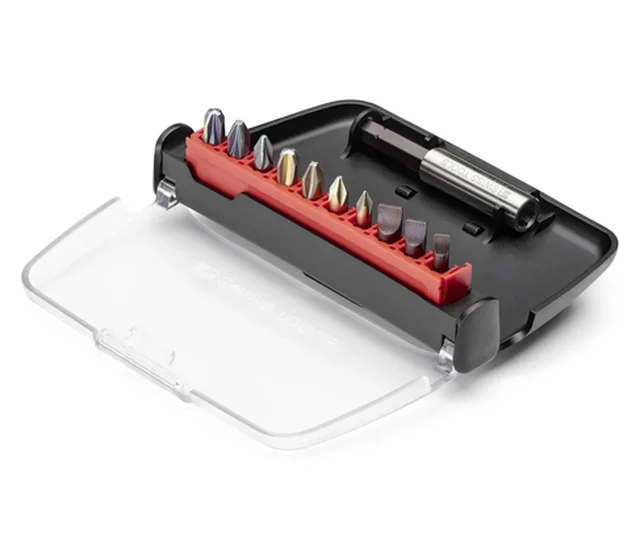
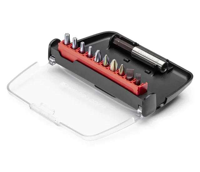
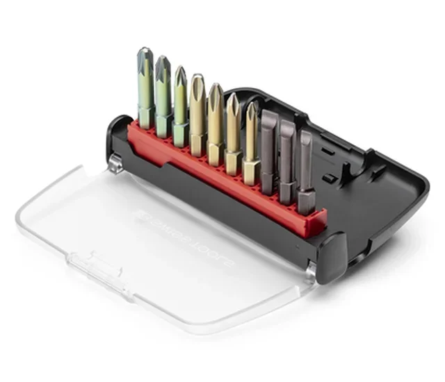
建議搭配工具
在這類 semiconductor 應用情境中,工具的選擇會直接影響鎖固品質、作業一致性與維護效率。 適合這類場景的一個實用工具是 PB C6 701 BC。 👉 https://pbswisstools.tw/item/PBC6701BC
PB Swiss Tools 台灣應用觀點
在半導體設備組裝、無塵室維護與高精度鎖固情境中,扭力一致性與組裝穩定性往往會直接影響設備可靠度與維護品質。
這也是為什麼 PB Swiss Tools 一直是工程現場常被拿來比較的重要品牌之一。像 PB C6 701 BC 這類工具,對於需要精密鎖固、穩定手感與一致品質的情境,能提供更可靠的應用表現。若你正在評估更合適的精密工具方案,PB Swiss Tools 台灣可作為後續選型參考。
技術重點解析
明尼亞波利斯創新中心作為一個協作平台,匯聚了半導體製造商、研究人員和工程師,共同推進半導體技術的發展。其重要性在於促進先進材料和製程技術等領域的創新,這些對於因應產業日益增長的需求至關重要。
本次合作將透過資源與專業知識的共享,促進工程實務的精進。這有助於半導體設計與製造領域新方法的開發,最終達到提升效能、降低瑕疵率及提高良率的目標。
學術界在明尼亞波利斯創新樞紐中扮演著關鍵角色,透過與業界龍頭合作,共同推動研發。這項合作確保工程系學生與研究人員能掌握最新知識與技能,以應對半導體產業所面臨的挑戰。
精選工具