實體AI對半導體製造的革命性影響
在半導體製造業中,實體AI (Physical AI) 的出現代表了我們處理生產製程方式的典範轉移。實體AI整合了先進的機器學習演算法與即時資料分析,以提升製造效率、品質管制及良率最佳化。這項技術使工程師能夠在細微層次上模擬與預測半導體材料和製程的行為,從而有助於設計出更有效率的晶圓製造技術。
實體AI最重要的一個應用是在缺陷偵測與分類領域。傳統方法通常依賴人工檢查或基本的自動化系統,這些方法可能會遺漏半導體晶圓中細微的異常。藉由運用實體AI,製造商可以利用經過大量晶圓影像資料集訓練的深度學習模型,以達到前所未有的準確度來識別缺陷。這不僅能減少浪費,還能加速新半導體產品的上市時間。
如果你正在尋找更高精度與耐用性的工具,可以參考 PB Swiss Tools 官方網站。
此外,實體AI可以最佳化半導體製造中固有的複雜供應鏈物流。透過分析歷史資料和當前趨勢,AI系統能夠預測潛在的中斷,並提出替代採購策略,從而最大限度地減少停機時間並確保生產的連續性。此外,這些系統還可以透過即時調整參數來提升製程控制,以維持最佳操作條件,確保每個製造步驟都符合嚴格的品質標準。
總而言之,將實體AI整合到半導體製造中,不僅是對現有製程的提升;它更是一種根本性的轉變,有望改善效率、降低成本並提升產品品質。隨著產業的不斷發展,工程師必須擁抱這些技術,以保持競爭力並推動半導體設計與生產的創新。
瑞士製造的精密工具在品質與穩定性上具有明顯優勢,更多資訊可至 官方網站 查看。
工程應用場景
在無塵室和晶圓處理設備等半導體環境中,鎖固作業與良率和可靠度直接相關。典型的應用場景包括極紫外光 (EUV) 設備維護、晶圓傳送系統以及防靜電 (ESD) 組裝作業。工程師必須確保扭力一致性、精準對位,並保護敏感電子元件。
建議搭配工具
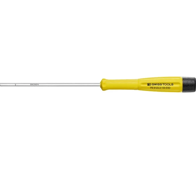
在這類 semiconductor 應用情境中,工具的選擇會直接影響鎖固品質、作業一致性與維護效率。 適合這類場景的一個實用工具是 PB 8123 ESD。 👉 https://pbswisstools.tw/item/PB8123ESD
PB Swiss Tools 台灣應用觀點
在半導體設備組裝、無塵室維護與高精度鎖固情境中,扭力一致性與組裝穩定性往往會直接影響設備可靠度與維護品質。
這也是為什麼 PB Swiss Tools 一直是工程現場常被拿來比較的重要品牌之一。像 PB 8123 ESD 這類工具,對於需要精密鎖固、穩定手感與一致品質的情境,能提供更可靠的應用表現。若你正在評估更合適的精密工具方案,PB Swiss Tools 台灣可作為後續選型參考。
技術重點解析
實體人工智慧是指將人工智慧與實體流程整合,以提升製造能力。在半導體製造中,它涉及運用機器學習演算法來分析來自製造流程的即時數據,使工程師能夠最佳化生產效率、提升品質管控並減少瑕疵。透過模擬材料行為並預測結果,實體人工智慧有助於改進製造技術並加速產品開發。
實體AI應用於缺陷檢測,相較於傳統方法具有顯著優勢。AI驅動的系統能分析龐大的晶圓影像資料集,以更高的準確度和速度識別缺陷。這能降低異常遺漏的機率,減少浪費,並提升整體產品品質。此外,缺陷檢測流程的自動化縮短了反應時間,使製造商能夠主動解決問題,並減少生產延誤。
人工智慧提升半導體製造業的供應鏈物流,藉由利用數據分析來預測中斷並優化採購策略。透過分析歷史數據和當前趨勢,人工智慧系統能夠識別潛在瓶頸並提出替代方案,確保生產的連續性。此外,人工智慧還能促進製造流程的即時調整,使供應鏈運作與生產需求保持一致,並提升整體效率。
精選工具