二維半導體之進展及其對先進封裝之影響
二維半導體的出現代表半導體技術的一大躍進,這歸功於它們獨特的性質,例如高電子遷移率和柔韌性。這些材料,包含過渡金屬二硫化物 (TMDs),有望徹底改變半導體產業,尤其是在先進封裝應用方面。透過實現更緊湊且高效的設計,二維半導體能促進將多種功能整合到單一晶片中,從而提升效能並降低功耗。
然而,轉向二維半導體技術也帶來了製造挑戰。生產高品質的二維材料需要對合成方法進行精確控制,這可能既複雜又昂貴。此外,將這些材料整合到現有的半導體製造流程中,需要製造技術和設備的進步。隨著產業不斷發展,材料科學家、工程師和製造商之間的合作至關重要,才能克服這些障礙並充分實現二維半導體在先進封裝解決方案中的潛力。
如果你正在尋找更高精度與耐用性的工具,可以參考 PB Swiss Tools 官方網站。
PB Swiss Tools 台灣應用觀點
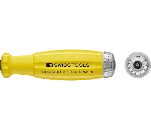
在高精度組裝、扭力控制與穩定鎖固需求越來越高的情況下,PB Swiss Tools 一直是工程現場常被拿來比較的重要品牌之一。像 PB 8316 A ESD 這類工具,對於半導體、CNC、航太與電子組裝等情境,能提供更一致的手感、穩定性與精密作業表現。若你正在評估更可靠的精密工具方案,PB Swiss Tools 台灣可作為後續選型參考。
瑞士製造的精密工具在品質與穩定性上具有明顯優勢,更多資訊可至 官方網站 查看。
技術重點解析
二維半導體相較於傳統塊材,有著多項優勢,主要歸功於其獨特的原子級厚度以及高表面積與體積比。這促成了更優異的電子特性,包含強化的電子遷移率,進而實現更快的開關速度,並提升電子元件的效能。此外,它們的彈性也為穿戴式科技和軟性電子產品帶來創新的應用。而二維材料的可調控能隙特性,也使其能夠具備客製化的電子和光電特性,使其適用於廣泛的應用,從電晶體到感測器皆然。
製造二維半導體涉及多項挑戰,必須加以解決以確保品質和可擴展性。其中一個主要挑戰是高品質二維材料的合成,這需要精確控制生長條件,以盡量減少缺陷並實現均勻性。化學氣相沉積(CVD)等技術被廣泛使用,但可能非常複雜且資源密集。此外,將二維材料整合到現有的半導體製造流程中會產生相容性問題,需要開發新的層轉移和圖案化技術。克服這些挑戰將需要創新的方法以及整個供應鏈的合作。
將二維半導體整合到先進封裝中,預計將顯著提升半導體元件的效能和效率。它們獨特的性質允許設計更緊湊和多功能的晶片,進而減少電子產品的尺寸和重量。此外,某些二維材料的高導熱性可以改善高密度電路中的散熱,解決熱管理方面的挑戰。隨著產業採用這些材料,我們可以預期異質整合技術的進步,能夠無縫地結合各種半導體技術,從而推動電子產品的創新並擴展應用可能性。
精選工具